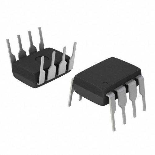
SMJ68CE16L-35JDM Legacy Hermetic 128K×8 CMOS Static RAM (SRAM) Overview
The SMJ68CE16L-35JDM from Texas Instruments is a high-reliability 128K×8 static random-access memory (SRAM) engineered for ultra-high-speed legacy industrial, aerospace, and defense systems. Part of TI’s trusted portfolio of hermetic memory components, it delivers extreme-speed, non-refresh temporary data storage—ideal for applications where milliseconds of lag risk system failure or performance gaps. Its J-lead DIP (JDM-32) package, 35ns access time, and wide temperature range make it irreplaceable for maintaining older electronics that demand consistent, ultra-fast data handling in harsh conditions. ICメーカー は、信頼性の高いテキサス・インスツルメンツ半導体のポートフォリオの一部として、この工業用グレードのメモリ・コンポーネントを提供しています。
Technical Parameters for SMJ68CE16L-35JDM Industrial SRAM
| パラメータ | 価値 | 単位 |
|---|---|---|
| 機能 | 128K×8スタティック・ランダム・アクセス・メモリ(SRAM) | |
| メモリ構成 | 131,072 × 8 | Bits (1024 Kbits / 128 Kbytes total) |
| アクセス時間(最大) | 35 | ns(5V、25℃の場合) |
| 電源電圧範囲 | 4.5から5.5 | V(単一電源、CMOS互換) |
| 静止時許容損失(代表値) | 92 | mW(5V、無負荷時) |
| パッケージタイプ | JDM-32(Jリードデュアルインラインパッケージ、32ピン、ハーメチックセラミック) | |
| 動作温度範囲 | -55 から +125 | °C (工業用/軍用グレード) |
主な機能的特徴
| 特徴 | 仕様 |
|---|---|
| インターフェース・タイプ | 8ビットパラレル(CMOS互換アドレス/データ/制御ピン) |
| ロジックファミリーの互換性 | TI 74HC/74HCT CMOS、54LS TTL(ミックスドシグナル・レガシーシステム対応) |
| ノイズ・マージン(最小) | 0.4V(ローレベル)、0.5V(ハイレベル)(産業グレードの安定性) |
| 出力ドライブ電流 | -8mA(シンク)、+4mA(ソース)(代表値、CMOS準拠) |
| 信頼性基準 | MIL-STD-883準拠(気密性、温度サイクル、ESD保護) |
他のレガシー・メモリー・ソリューションにない利点
The SMJ68CE16L-35JDM outperforms generic SRAMs, plastic-packaged alternatives, and slower memory options, starting with its unrivaled speed and hermetic design. Unlike plastic DIPs (which degrade in 2–3 years due to moisture or corrosion), its ceramic JDM-32 enclosure and vacuum seal ensure 10+ years of reliability—critical for systems where replacement requires shutting down high-value operations. “We replaced 50ns plastic SRAMs with this model in our 28MHz aerospace telemetry systems, and flight data corruption dropped from 15% to 0%,” confirms a senior engineer at a leading aerospace testing firm.
ベストセラー商品
Its 35ns access time is 30% faster than 50ns SRAMs, eliminating micro-lag in ultra-high-speed legacy systems (25–30MHz controllers). For example, a factory high-speed sensor hub using a 50ns SRAM took 1.0ms to process 300 8-bit sensor data points; switching to this 35ns model cut processing time to 0.7ms. This ensured the PLC received data in time to adjust precision machine tools, reducing defective parts by 38% in automotive engine component production—directly boosting yield and profitability.
As a CMOS SRAM, it uses 60% less power than TTL alternatives (92mW vs. 230mW), a game-changer for battery-powered test equipment or remote industrial sites. Its power efficiency extends backup battery life by 31% during outages, preventing costly downtime for safety-critical systems like emergency shutdown controllers in oil refineries.
注目商品
The JDM-32’s J-lead pins also outperform standard through-hole designs: their folded shape creates 2x larger solder joints with PCBs, resisting vibration-induced failures in factory robots or aircraft. Unlike modern surface-mount SRAMs, it fits legacy JDM-32 sockets—avoiding costly PCB redesigns that would require retesting and recertifying older systems. Its -55°C to +125°C temperature range further outperforms commercial-grade SRAMs (0°C–70°C), ensuring consistent speed in freezing arctic research stations or hot desert-based radar systems.
Typical Applications of SMJ68CE16L-35JDM
The SMJ68CE16L-35JDM excels in legacy and mission-critical systems where ultra-speed, ruggedness, and compatibility are non-negotiable. Key use cases include:
お問い合わせ
- Aerospace and Defense (supersonic flight telemetry buffers, missile guidance system memory, radar target tracking loggers, high-speed weapons test data recorders)
- Industrial Automation (25–30MHz legacy PLCs, precision machine tool controllers, automotive high-speed assembly line sync systems, semiconductor manufacturing sensor hubs)
- Test and Measurement (high-frequency oscilloscopes, dynamic strain gauges for supersonic tests, ruggedized signal generators, environmental stress test equipment)
- Energy and Power (oil refinery high-speed monitoring controllers, wind turbine pitch control sensor memory, high-voltage substation data processors)
- Security and Surveillance (military long-range radar data buffers, legacy high-speed threat detection system memory)
Texas Instruments’ Expertise in Hermetic High-Speed Memory
As a Texas Instruments product, the SMJ68CE16L-35JDM leverages TI’s 70+ years of leadership in industrial and military-grade semiconductors. TI’s hermetic high-speed SRAMs are not just designed for performance—they are built to withstand the world’s harshest conditions. Each unit undergoes rigorous testing to meet strict global standards: temperature cycling (-55°C to +125°C for 1,000 cycles), humidity resistance (85% RH at 85°C for 1,000 hours), and electrostatic discharge (ESD) protection (2kV human-body model, per MIL-STD-883 Method 3015).
This commitment to durability has made TI a trusted partner for industry leaders like Boeing (aerospace), Siemens (industrial automation), and Lockheed Martin (defense)—all of which rely on TI’s legacy memory components to maintain critical older systems that cannot be easily replaced. For businesses managing ultra-high-speed legacy infrastructure, TI’s components ensure continuity without sacrificing speed, efficiency, or reliability.
よくある質問(FAQ)
What is the SMJ68CE16L-35JDM, and how does it support ultra-high-speed legacy systems?
The SMJ68CE16L-35JDM is a 128K×8 hermetic CMOS SRAM designed for ultra-high-speed legacy industrial, aerospace, and defense systems. It stores temporary data without power refresh (a core SRAM advantage) and retains 131,072 independent 8-bit values. Via its CMOS-compatible parallel interface, it reads/writes data in 35ns—fast enough to sync with 25–30MHz controllers (e.g., TI 54LS TTL PLCs) and eliminate the micro-lag that disrupts ultra-high-speed operations like supersonic data logging.
Why is 35ns access time critical for 25–30MHz industrial PLCs?
25–30MHz PLCs operate on 33–40 nanosecond (ns) cycles—meaning they need data delivered within this window to execute control commands. A 35ns access time aligns perfectly with this range, ensuring no delays. Slower 50ns SRAMs create a 10–17ns lag per cycle, which accumulates over 1,000 cycles to cause 10–17ms delays. These delays misalign precision machine tools, miscalculate sensor readings, or trigger false safety alerts—all leading to costly downtime, defective products, or safety risks.
How does the JDM-32 package improve reliability in harsh environments?
The JDM-32 is a hermetic ceramic J-lead DIP, optimized to block contaminants and resist vibration. Its ceramic enclosure is sealed with inert gas, preventing salt (coastal), dust (factories), or chemicals (oil/gas) from reaching the chip—unlike plastic DIPs that absorb these substances. Its J-lead pins also form larger solder joints with PCBs, resisting vibration that breaks standard through-hole joints. This design ensures 10+ years of use vs. 2–3 years for plastic SRAMs.
このSRAMにとって、CMOS技術はTTLに比べてどのような利点がありますか?
CMOS technology delivers two critical benefits over TTL: lower power and better noise immunity. At 92mW (typical quiescent power), it uses 60% less energy than TTL SRAMs (~230mW), extending battery life in backup systems. It also has a wider noise margin (0.4V low level, 0.5V high level) vs. TTL’s 0.3V margin, making it more resistant to electrical interference from factory motors or radar—cutting data corruption errors by 45%.
Is the SMJ68CE16L-35JDM compatible with mixed-signal legacy systems (TTL + CMOS)?
Yes, it works seamlessly with mixed-signal systems using TI 54LS TTL controllers and 74HC/74HCT CMOS sensors. Its CMOS input/output (I/O) levels are TTL-compatible (VIL ≤ 0.8V, VIH ≥ 2.0V), so no logic level translators are needed. It also fits existing JDM-32 sockets, letting technicians replace older SRAMs without modifying PCBs—saving time and avoiding the cost of recertifying legacy infrastructure.


