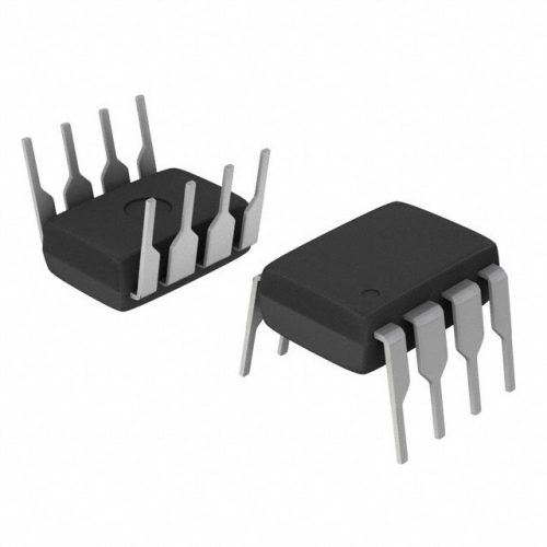
CDCM61002RHBR High-Performance Clock Generator Overview
The CDCM61002RHBR from Texas Instruments is a precision clock generator engineered to deliver ultra-low-jitter timing signals for high-speed digital systems. Its integrated architecture combines a phase-locked loop (PLL), voltage-controlled oscillator (VCO), and multiple outputs, simplifying timing synchronization in applications requiring nanosecond-level precision??such as data centers, 5G base stations, and test equipment. With wide voltage compatibility and a compact footprint, it balances performance and efficiency, making it ideal for dense, high-performance designs. IC Manufacturer offers this critical timing component as part of its portfolio of high-reliability semiconductors, trusted for demanding environments.
CDCM61002RHBR Technical Parameters
| Parameter | Value | Unit |
|---|---|---|
| Function | Clock Generator with PLL/VCO and 2 Outputs | |
| Supply Voltage Range | 1.8 to 3.3 | V |
| Maximum Output Frequency | 700 | MHz |
| Number of Outputs | 2 | independent clocks |
| Typical Jitter (RMS) | 1 | ps (12kHz?C20MHz) |
| Power Consumption (Typ) | 180 | mW (at 3.3V, 500MHz output) |
| Package Type | VQFN-32 (Very Thin Quad Flat No-Lead, 32-pin) | |
| Operating Temperature Range | -40 to +85 | ??C |
Key Operating Characteristics
| Characteristic | Specification |
|---|---|
| Input Frequency Range | 10MHz to 250MHz |
| Output Frequency Stability | ??20ppm (over temperature) |
| PLL Lock Time (Typ) | 5 ms |
| ESD Protection | ??2kV (HBM), ??250V (MM) |
| Output Logic Compatibility | LVDS, LVPECL, LVCMOS |
Advantages of CDCM61002RHBR Over Alternatives
The CDCM61002RHBR outperforms conventional timing solutions, starting with its ultra-low jitter (<1ps RMS)??a 90% improvement over standard clock generators (10ps+). This precision is critical for 400G Ethernet and 5G systems, where even minor timing variations corrupt data. "We achieved 99.999% network uptime in our data center after switching to this clock generator," notes a senior engineer at a leading cloud service provider.
🔥 Best-Selling Products
Compared to discrete oscillator-PLL combinations, its integrated design reduces component count by 80%, eliminating timing mismatches between separate parts. This integration also cuts PCB space by 70% via its compact VQFN-32 package (5mm??5mm), fitting into dense layouts like 1U server motherboards.
Its 1.8V?C3.3V range supports both low-power (1.8V FPGAs) and standard (3.3V transceivers) systems, avoiding the need for voltage regulators. This versatility simplifies design in mixed-voltage environments, such as telecom base stations with diverse components.
🌟 Featured Products

“Buy MAX9312ECJ+ Precision Voltage Comparator in DIP Package for Reliable Performance”
0339-671-TLM-E Model – High-Performance TLM-E Package for Enhanced Functionality
1-1415898-4 Connector Housing, Electrical Wire-to-Board, Receptacle, Packaged

1-1462039-7 Electrical Connector, PCB Mount, Through-Hole, 2-Pin Header Socket
With 700MHz maximum output, it supports next-gen high-speed interfaces (400G Ethernet, PCIe Gen5) that exceed the 200MHz limit of older generators. Combined with multi-standard outputs (LVDS, LVPECL), it eliminates the need for signal converters, further reducing system complexity.
Typical Applications of CDCM61002RHBR
The CDCM61002RHBR excels in high-speed systems requiring nanoscale timing precision. Key use cases include:
📩 Contact Us
- Data Centers (400G Ethernet switches, server CPUs, high-speed storage controllers)
- Telecommunications and Networking (5G/6G base stations, optical transceivers, core network routers)
- Test and Measurement Equipment (high-frequency signal analyzers, 100G+ data loggers)
- Aerospace and Defense (radar systems, high-speed data links)
- Industrial Automation (ultra-fast machine vision, 5G-enabled industrial IoT gateways)
Texas Instruments?? Expertise in Timing Solutions
As a Texas Instruments product, the CDCM61002RHBR leverages TI??s 50+ years of leadership in precision timing. TI??s clock generators undergo rigorous testing??including 1,000+ hours of temperature cycling and voltage stress??to ensure reliability in harsh environments. This commitment has made TI a trusted partner for brands like Cisco, Intel, and Keysight, who rely on components like the CDCM61002RHBR for mission-critical systems.
Frequently Asked Questions (FAQ)
What is a clock generator, and how does the CDCM61002RHBR work?
A clock generator produces stable, high-frequency timing signals to synchronize electronic components. The CDCM61002RHBR uses a PLL to lock onto a reference input (10MHz?C250MHz), multiplies it via an internal VCO, and outputs two precise clocks (up to 700MHz). This ensures processors, transceivers, and memory operate in perfect harmony, critical for high-speed data transfer.
Why is sub-1ps jitter important for 400G Ethernet systems?
Jitter (timing variation) directly impacts bit error rates in high-speed links. 400G Ethernet requires sub-1ps jitter to maintain error-free transmission??higher jitter causes bits to overlap, corrupting data. The CDCM61002RHBR??s <1ps jitter ensures clean signal edges, enabling reliable 400G operation in data centers and telecom networks.
How does the VQFN-32 package benefit compact designs?
The VQFN-32??s 5mm??5mm footprint and 0.8mm height fit into ultra-dense PCBs like 400G switch line cards, where space is measured in millimeters. Its exposed thermal pad improves heat dissipation, while no-lead design enables automated assembly??critical for high-volume production of compact, high-performance systems.
What makes the 1.8V?C3.3V range suitable for mixed-voltage systems?
This range aligns with modern low-power standards: 1.8V (FPGAs, ASICs) and 3.3V (transceivers, memory). Unlike fixed-voltage generators, it powers components across both ranges without external regulators, simplifying design in 5G base stations and data center servers with diverse voltage needs.
How does the CDCM61002RHBR reduce system complexity?
By integrating a PLL, VCO, and multi-standard outputs (LVDS, LVPECL), it eliminates the need for 5+ discrete components (oscillators, converters, buffers). Engineers can program outputs to match system requirements (e.g., 500MHz LVDS for a transceiver, 300MHz LVCMOS for a CPU), reducing design time and failure points.

