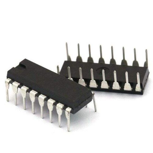
CY7C1021V33-15VCT Overview
The CY7C1021V33-15VCT is a high-performance static RAM (SRAM) device designed for fast, reliable memory storage in industrial and embedded systems. Offering a 1M-bit density organized as 131,072 words by 8 bits, it operates at a 15 ns access time and supports low power operation with a 3.3V power supply. This SRAM supports asynchronous read and write operations with separate control signals for easy interfacing. Its compact 44-pin TSOP II package optimizes board space while maintaining signal integrity. Engineers and sourcing specialists will find this device well-suited for applications requiring fast, stable memory with minimal latency and power consumption. For more detailed information, please visit Fabricante de CI.
CY7C1021V33-15VCT Technical Specifications
| Parámetro | Especificación |
|---|---|
| Densidad de memoria | 1M bit (131,072 x 8) |
| Tiempo de acceso | 15 ns |
| Tensión de funcionamiento | 3.3 V ?? 0.3 V |
| Tipo de envase | 44-pin TSOP II |
| Tensión de conservación de los datos | 2,0 V (mínimo) |
| Temperatura de funcionamiento | 0??C to +70??C |
| Corriente de espera | 10 ??A (typical) |
| Input/Output Configuration | Asynchronous, separate WE, OE, CE controls |
CY7C1021V33-15VCT Key Features
- Fast 15 ns access time: Enables high-speed data retrieval, minimizing system latency in performance-critical applications.
- Low-voltage 3.3 V operation: Reduces power consumption and heat generation, suitable for low-power embedded designs.
- Asynchronous operation with separate control signals: Provides flexible read and write cycles, simplifying timing design and increasing system efficiency.
- Compact 44-pin TSOP II package: Saves PCB space while maintaining excellent signal quality and ease of mounting.
CY7C1021V33-15VCT Advantages vs Typical Alternatives
This SRAM device offers a superior balance of speed, power efficiency, and density compared to typical asynchronous SRAMs operating at higher voltages or slower speeds. Its 3.3 V operation reduces power draw significantly, while the 15 ns access time improves throughput and responsiveness. The separate control signals for write enable, output enable, and chip enable enhance integration flexibility and system reliability, making it a preferred choice for engineers seeking robust memory solutions in embedded and industrial contexts.
Productos más vendidos
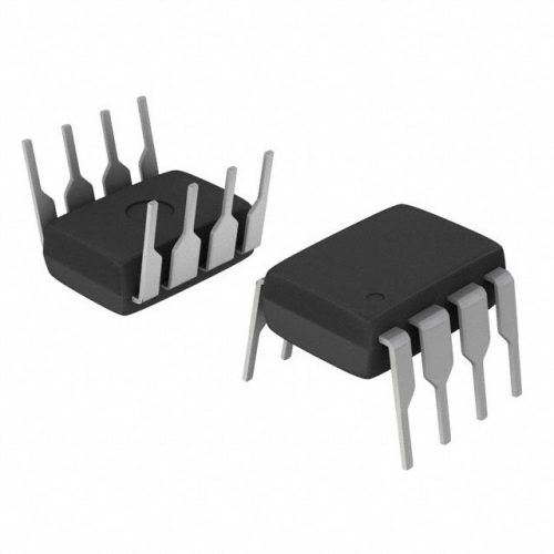
TLC555 Timer IC - Temporizador de precisión de Texas Instruments en encapsulado PDIP-8

Texas Instruments TL081 Op Amp de entrada JFET de bajo ruido - encapsulado DIP-8

Texas Instruments UC3842 Controlador PWM de modo de corriente - Paquete DIP-8

Texas Instruments LM2937 Regulador de voltaje encapsulado TO-220 - Lineal de baja caída
Aplicaciones típicas
- Embedded system memory: Ideal for buffering and temporary storage in microcontroller- and DSP-based designs requiring fast access times and low power consumption.
- Networking equipment: Suitable for packet buffering and data caching in routers and switches demanding rapid data throughput.
- Telecommunications: Provides reliable storage for high-speed data processing in base stations and communication controllers.
- Industrial control systems: Supports fast access to control parameters and real-time data logs in automation and instrumentation devices.
CY7C1021V33-15VCT Brand Info
The CY7C1021V33-15VCT is a product from a reputable semiconductor manufacturer specializing in high-quality memory ICs. This device represents a mature solution in the asynchronous SRAM market, combining proven architecture with modern low-voltage operation. It is designed to meet the stringent demands of industrial and embedded applications, ensuring long-term reliability, consistent performance, and ease of integration. The brand behind this product is recognized for its commitment to high manufacturing standards and comprehensive technical support.
PREGUNTAS FRECUENTES
What is the primary interface type of this SRAM device?
This SRAM uses an asynchronous interface with separate control signals for write enable (WE), output enable (OE), and chip enable (CE). This allows independent control of read and write operations without requiring a clock, simplifying integration in various digital systems.
Productos destacados

"Compre el comparador de tensión de precisión MAX9312ECJ+ en encapsulado DIP para un rendimiento fiable"
Modelo 0339-671-TLM-E - Paquete TLM-E de alto rendimiento para una funcionalidad mejorada
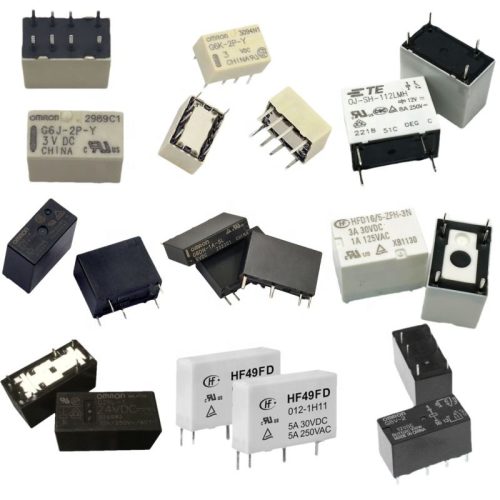
1-1415898-4 Connector Housing, Electrical Wire-to-Board, Receptacle, Packaged

1-1462039-7 Electrical Connector, PCB Mount, Through-Hole, 2-Pin Header Socket
What power supply voltage does this memory chip require?
En

