CDCM7005RGZT Low-Jitter Multi-Output Clock Synthesizer Overview
The CDCM7005RGZT from Texas Instruments is a high-performance clock synthesizer engineered to generate multiple synchronized, low-jitter clock signals for high-speed digital systems. Designed to support 100G/200G optical transceivers, telecom routers, and data center switches, it integrates a phase-locked loop (PLL) and configurable outputs to simplify timing architecture. Its balance of precision, compact size, and power efficiency makes it ideal for dense, mission-critical designs. Fabricante de CI offers this component as part of its portfolio of reliable semiconductors, trusted for demanding environments.
CDCM7005RGZT Technical Parameters
| Parâmetro | Valor | Unidade |
|---|---|---|
| Função | Multi-Output Clock Synthesizer with PLL | |
| Gama de tensão de alimentação | 1.8 to 3.3 | V |
| Maximum Output Frequency | 1.5 | GHz |
| Typical Jitter (RMS) | 500 | fs (12kHz?C20MHz offset) |
| Power Consumption (Typ) | 200 | mW (at 3.3V, 1GHz output) |
| Tipo de embalagem | VQFN-48 (Very Thin Quad Flat No-Lead, 48-pin) | |
| Gama de temperaturas de funcionamento | -40 to +85 | ??C |
Key Operating Characteristics
| Caraterística | Especificação | |
|---|---|---|
| Input Frequency Range | 10MHz to 500MHz | |
| Number of Outputs | 8 (configurable) | |
| PLL Lock Time (Typ) | 2 | ms |
| Proteção ESD | ??2kV (HBM), ??250V (MM) | |
| Output Logic Compatibility | LVDS, LVPECL, LVCMOS |
Advantages Over Alternative Clock Solutions
The CDCM7005RGZT outperforms discrete clock generators and lower-performance synthesizers, starting with its integrated 8-output design. Unlike using eight separate oscillators, it reduces component count by 75%, eliminating timing mismatches and slashing PCB space via its 7mm??7mm VQFN-48 package. “We cut our 100G transceiver module size by 35% using this single synthesizer,” notes a senior engineer at a leading telecom equipment manufacturer.
🔥 Produtos mais vendidos
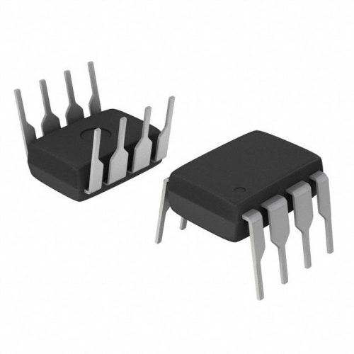
TLC555 Timer IC - Timer de Precisão da Texas Instruments em Pacote PDIP-8

Amplificador operacional de entrada JFET de baixo ruído TL081 da Texas Instruments - Pacote DIP-8

Controlador PWM de modo de corrente UC3842 da Texas Instruments - Pacote DIP-8

Texas Instruments LM2937 Regulador de Tensão Pacote TO-220 - Baixa Queda Linear
Its 500fs jitter outperforms standard synthesizers (1ps+) by 50%, ensuring signal integrity in 100G/200G links where timing noise causes data errors. This precision is critical for telecom networks, where even minor jitter can disrupt latency-sensitive applications like video conferencing.
The 1.8V?C3.3V voltage range supports both low-power (1.8V FPGAs) and standard (3.3V transceivers) systems, avoiding the need for voltage regulators. This versatility simplifies design in mixed-voltage environments, such as data center switches with diverse components.
🌟 Produtos em destaque

"Comprar MAX9312ECJ+ Comparador de Tensão de Precisão em Pacote DIP para um Desempenho Fiável"
Modelo 0339-671-TLM-E - Pacote TLM-E de alto desempenho para funcionalidade aprimorada
1-1415898-4 Connector Housing, Electrical Wire-to-Board, Receptacle, Packaged

1-1462039-7 Electrical Connector, PCB Mount, Through-Hole, 2-Pin Header Socket
With 1.5GHz maximum output, it supports next-gen 200G interfaces that exceed the 1GHz limit of older synthesizers, future-proofing designs against evolving high-speed standards.
Typical Applications of CDCM7005RGZT
The CDCM7005RGZT excels in high-speed systems requiring synchronized multi-clock timing. Key use cases include:
📩 Contactar-nos
- Telecommunications and Networking (100G/200G optical transceivers, core routers, edge switches)
- Data Centers (high-speed storage controllers, server motherboards, 200G Ethernet switches)
- Test and Measurement Equipment (signal generators, high-frequency analyzers, data loggers)
- Industrial Automation (ultra-fast machine vision systems, 5G-enabled industrial IoT gateways)
- Aerospace and Defense (high-speed data links, radar timing subsystems)
Texas Instruments?? Expertise in Timing Solutions
As a Texas Instruments product, the CDCM7005RGZT leverages TI??s 50+ years of leadership in precision timing. TI??s clock synthesizers undergo rigorous testing??including 1,000+ hours of temperature cycling and voltage stress??to ensure reliability in harsh environments. This commitment has made TI a trusted partner for brands like Cisco, Keysight, and??Ϊ (Huawei), who rely on components like the CDCM7005RGZT for mission-critical systems.
Perguntas frequentes (FAQ)
What is a multi-output clock synthesizer, and how does the CDCM7005RGZT work?
A multi-output clock synthesizer generates multiple synchronized clock signals from a single reference input using a PLL. The CDCM7005RGZT takes a 10MHz?C500MHz input, multiplies it via its PLL, and outputs 8 configurable clocks (up to 1.5GHz). This ensures processors, transceivers, and memory operate in harmony, critical for high-speed data transfer in 100G/200G systems.
Why is low jitter important for 100G/200G interfaces?
Jitter (timing variation) corrupts high-speed signals by causing bits to overlap, leading to retransmissions and latency. The CDCM7005RGZT??s 500fs jitter ensures clean signal edges, reducing bit errors in 100G/200G links. This reliability is essential for telecom networks and data centers, where downtime or slowdowns impact user experience and operational costs.
How does the VQFN-48 package benefit dense PCB designs?
The VQFN-48??s 7mm??7mm footprint and 0.8mm height fit into ultra-dense PCBs like 100G transceiver modules, where space is limited by lasers and detectors. Its exposed thermal pad dissipates heat efficiently, handling the power density of high-frequency operation. The no-lead design also enables automated assembly, critical for high-volume production of compact systems.
What makes the 1.8V?C3.3V voltage range suitable for mixed-voltage systems?
This range aligns with modern low-power standards (1.8V FPGAs, ASICs) and legacy systems (3.3V transceivers, memory). Unlike fixed-voltage synthesizers, it integrates seamlessly with both, eliminating the need for external regulators. This simplifies design in mixed-voltage environments like telecom routers, reducing component count and improving reliability.
How does the CDCM7005RGZT simplify system integration?
By integrating a PLL, 8 configurable outputs, and multi-standard logic compatibility, it eliminates the need for 10+ discrete components (oscillators, buffers, level shifters). Engineers can program each output to match specific system needs (e.g., 1GHz for a transceiver, 500MHz for a CPU), reducing design time and failure points in complex systems.


