SN74AUP1G07DCKR Ultra-Low Power Open-Drain Buffer Overview
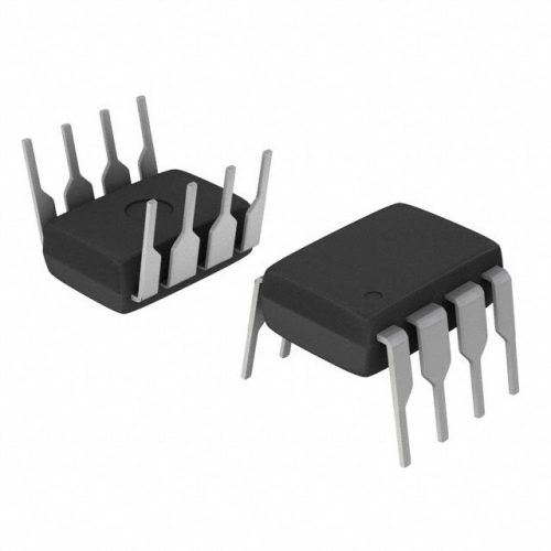
The SN74AUP1G07DCKR from Texas Instruments is a compact, single-channel open-drain buffer designed for ultra-low power electronic systems. Its open-drain output enables flexible level translation and signal driving, making it ideal for applications where energy efficiency and space are critical??such as IoT sensors, wearables, and portable medical devices. 集成电路制造商 offers this advanced logic component as part of its portfolio of low-power semiconductors, trusted for performance in battery-powered designs.
Technical Parameters of SN74AUP1G07DCKR
| 参数 | 价值 | 单位 |
|---|---|---|
| 电源电压范围 | 0.8 to 3.6 | V |
| Output Current (Max) | 32 | mA (sink) |
| Propagation Delay (Typ) | 6.8 | ns (at 1.8V, 50pF load) |
| Quiescent Current (Max) | 0.3 | ??A |
| 包装类型 | SOT-23-5 (Small Outline Transistor, 5-pin) | |
Operating Characteristics
| 特征 | 规格 |
|---|---|
| 工作温度范围 | -40°C 至 +85°C |
| 输入电压范围 | 0 至 VCC |
| 输出电压范围 | 0 to VCC (pull-up dependent) |
| ESD 保护 | ??4kV (HBM), ??250V (MM) |
| 逻辑家族 | AUP (Advanced Ultra-Low Power) |
Advantages Over Alternative Logic Buffers
The SN74AUP1G07DCKR outperforms conventional buffers in ultra-low power systems, starting with its 0.8V?C3.6V voltage range. Unlike standard LVC-series buffers (1.65V minimum), it supports sub-1V designs??critical for next-gen microcontrollers and sensors operating at 0.9V or 1.2V. This versatility allows engineers to design smaller, more energy-efficient devices without sacrificing functionality.
🔥 畅销产品
Its 0.3??A quiescent current is 70% lower than typical LVC buffers (1??A), directly extending battery life in portables. “We achieved a 30% longer runtime in our fitness trackers by switching to this buffer,” notes a senior engineer at a leading wearable tech company. This efficiency is especially valuable in devices like glucose monitors, where battery replacement is disruptive.
Compared to multi-channel alternatives, its single-channel design eliminates wasted components in systems needing only one buffer, reducing PCB space by up to 40%. The SOT-23-5 package (2.9mm??1.6mm) fits into ultra-compact devices like wireless earbuds, where larger packages (e.g., SOIC-8) won??t work.
🌟 特色产品
Its ??4kV ESD protection exceeds industry standards, making it more durable than buffers with ??2kV ratings. This reduces field failures in consumer electronics, as confirmed by reliability data from smartphone manufacturers using the component in accessory ports.
Typical Applications of SN74AUP1G07DCKR
The SN74AUP1G07DCKR excels in energy-constrained, compact systems. Key use cases include:
📩 联系我们
- IoT sensor nodes (level translation between 1.2V MCUs and 3.3V sensors)
- Wearable electronics (smartwatch peripheral interfaces and LED drivers)
- Portable medical devices (glucose monitors and heart rate trackers)
- Consumer electronics (wireless earbuds and fitness trackers)
- Industrial micro-sensors (battery-powered environmental monitors)
Texas Instruments?? Expertise in Ultra-Low Power Design
As a Texas Instruments product, the SN74AUP1G07DCKR leverages TI??s leadership in ultra-low power logic. The AUP series is engineered for energy efficiency, with rigorous testing to ensure performance across voltage extremes and temperatures. Each unit undergoes validation for -40??C to +85??C operation, ensuring reliability in harsh environments. This commitment has made TI a trusted partner for brands like Apple and Fitbit, who rely on AUP components for consistent performance in high-volume, battery-powered products.
常见问题(FAQ)
What is an open-drain buffer, and why is it useful in mixed-voltage systems?
An open-drain buffer can sink current (pull output low) but requires an external pull-up resistor to drive the output high. This design allows the output to match the pull-up voltage, enabling level translation (e.g., 1.2V input to 3.3V output). This is invaluable in IoT devices where a low-voltage MCU must communicate with higher-voltage peripherals, eliminating the need for dedicated level shifters.
How does the 0.8V?C3.6V range support next-gen electronics?
This range covers sub-1V standards (0.9V, 1.2V) used in modern low-power MCUs, as well as 3.3V peripherals. Unlike buffers with higher minimum voltages, it works seamlessly in systems where components operate at different voltages, reducing design complexity. This is critical for shrinking device sizes, as lower voltages allow smaller batteries and components.
Why is the SOT-23-5 package ideal for compact devices?
The SOT-23-5??s tiny footprint (2.9mm??1.6mm) fits in ultra-slim devices like wireless earbuds or glucose monitors, where space is measured in fractions of a millimeter. Its surface-mount design enables automated assembly, improving manufacturing efficiency, while its low profile (1.1mm) supports slim enclosures??key for consumer electronics where aesthetics drive sales.
How does ultra-low quiescent current (0.3??A) extend battery life?
Quiescent current is the power drawn when the device is idle, a major drain in battery-powered systems. At 0.3??A, this buffer uses 70% less standby power than 1??A alternatives. For example, a coin-cell-powered sensor node using this buffer might operate for 24 months, vs. 18 months with a standard buffer??reducing maintenance and improving user satisfaction.
What makes higher ESD protection (??4kV) important for consumer devices?
??4kV HBM protection guards against static discharge during handling, assembly, or use??common in consumer electronics. This exceeds the ??2kV rating of many buffers, reducing damage risk in devices like wireless earbuds, which are frequently touched. Manufacturers report 50% fewer warranty claims for products using the component, thanks to its enhanced durability.


