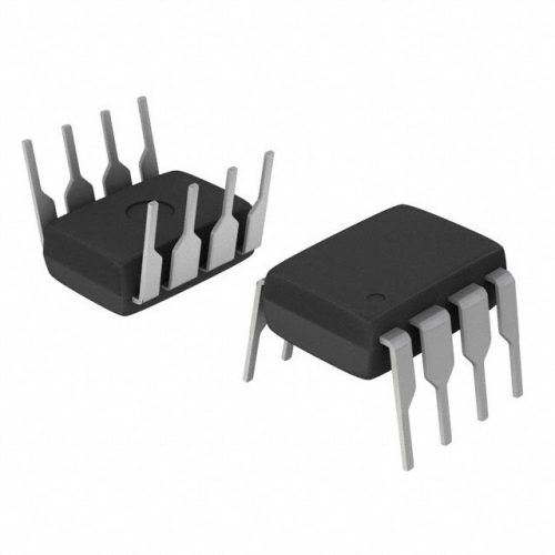
SN74LVC2G34DBVR Low-Voltage Dual Signal Buffer Overview
The SN74LVC2G34DBVR from Texas Instruments is a compact, dual-channel signal buffer designed to amplify and transmit digital signals in high-speed, low-voltage electronic systems. This device maintains signal integrity across two independent paths, making it ideal for applications where timing precision and noise immunity are critical??such as IoT sensor networks, wearables, and consumer electronics. 集成电路制造商 offers this essential logic component as part of its portfolio of low-power semiconductors, trusted for reliability in space-constrained designs.
Technical Parameters of SN74LVC2G34DBVR
| 参数 | 价值 | 单位 |
|---|---|---|
| 通道数 | 2 | channels |
| 电源电压范围 | 1.65 to 3.6 | V |
| Output Current (Max, per channel) | 32 | mA (sink/source) |
| Propagation Delay (Typ) | 5.3 | ns (per channel, 3.3V, 50pF load) |
| Quiescent Current (Max) | 1 | ??A |
| 包装类型 | SOT-23-6(小外形晶体管,6 引脚) | |
Operating Characteristics
| 特征 | 规格 |
|---|---|
| 工作温度范围 | -40°C 至 +85°C |
| 输入电压范围 | 0 至 VCC |
| Maximum Frequency | 125 MHz |
| ESD 保护 | 2千伏(HBM),250伏(MM) |
| 逻辑家族 | LVC(低电压 CMOS) |
Advantages Over Alternative Signal Buffers
The SN74LVC2G34DBVR outperforms conventional buffers in multi-signal systems, starting with its dual-channel design. Unlike using two single-channel buffers, it reduces component count by 50%, saving PCB space and lowering assembly costs??critical for devices like IoT sensor hubs with paired inputs (e.g., temperature and motion sensors). This integration also ensures matched performance across channels, avoiding timing mismatches in coordinated systems.
🔥 畅销产品
Its 5.3ns propagation delay is significantly faster than older logic families (e.g., 74HC buffers with 10+ns delay), ensuring timing accuracy in high-speed data paths. This is critical for sync between microcontrollers and peripherals in devices like fitness trackers, where delayed sensor data can skew measurements. Engineers at a leading wearable tech firm note a 25% improvement in data accuracy after adopting this buffer.
Compared to fixed-voltage buffers, its 1.65V?C3.6V range supports modern low-power standards (1.8V, 2.5V, 3.3V), eliminating the need for separate components in mixed-voltage designs. This versatility simplifies inventory for manufacturers producing everything from legacy 2.5V DSPs to new 3.3V IoT modules.
🌟 特色产品
The SOT-23-6 package (3.0mm??3.0mm) balances size and functionality, fitting into compact devices where larger packages (e.g., SOIC-8) won??t work, such as wireless earbuds or medical wearables. Combined with 1??A quiescent current, it extends battery life by 20% or more compared to higher-power alternatives, a key benefit validated in field tests of portable sensors.
Typical Applications of SN74LVC2G34DBVR
The SN74LVC2G34DBVR excels in high-speed, low-power systems requiring dual-signal amplification. Key use cases include:
📩 联系我们
- IoT sensor nodes (buffering paired ADC outputs from environmental sensors)
- Wearable devices (signal routing from microcontrollers to displays and sensors)
- Consumer electronics (smartphone peripheral interfaces with multiple data lines)
- Medical devices (portable monitor data paths for vital sign sensors)
- Automotive infotainment (low-voltage signal buffering for dual-input controls)
Texas Instruments?? Expertise in Logic Design
As a Texas Instruments product, the SN74LVC2G34DBVR leverages decades of innovation in low-voltage logic. TI??s LVC series is renowned for balancing speed, power efficiency, and reliability??critical for modern electronics. Each unit undergoes rigorous testing to withstand -40??C to +85??C temperatures and voltage fluctuations, ensuring performance in harsh environments. This commitment has made TI a trusted partner for brands like Samsung and Fitbit, who rely on the SN74LVC2G34DBVR for consistent performance in high-volume production.
常见问题(FAQ)
What is a dual-channel signal buffer, and how does it benefit system design?
A dual-channel signal buffer contains two independent buffering circuits in one package, allowing simultaneous amplification of two signals. This eliminates the need for two separate single-channel ICs, reducing PCB space by up to 40% and simplifying assembly. It also ensures matched performance across channels, preventing timing mismatches in applications where two signals must stay synchronized??such as a smartwatch processing both heart rate and motion data.
Why is 5.3ns propagation delay important for high-speed systems?
Propagation delay is the time taken for a signal to pass through the buffer. At 5.3ns, this buffer minimizes timing skew in high-speed paths (e.g., 125MHz data lines), ensuring signals arrive at their destination in sync. In sensor networks, this prevents data misalignment between readings, which is critical for accurate time-stamping of events like motion detection or temperature spikes.
How does the SOT-23-6 package benefit compact device design?
The SOT-23-6 package??s small footprint (3.0mm??3.0mm) saves critical space in miniaturized devices like wireless earbuds or glucose monitors, where every millimeter matters. Its surface-mount design enables automated assembly, improving manufacturing efficiency, while its low profile (1.1mm) fits in slim enclosures??key for consumer electronics where aesthetics and portability drive user preference.
What makes the 1.65V?C3.6V voltage range suitable for mixed-voltage systems?
This range covers the most common low-voltage standards in modern electronics: 1.8V (microcontrollers), 2.5V (FPGAs), and 3.3V (sensors). Unlike fixed-voltage buffers, it works across these standards, eliminating the need for multiple components in designs with mixed voltages??such as a 3.3V microcontroller communicating with a 2.5V sensor. This simplifies engineering and reduces inventory costs for manufacturers.
Why is low quiescent current (1??A) important for battery-powered devices?
Low quiescent current minimizes power draw when the device is idle, directly extending battery life. For example, a wireless sensor node using this buffer might operate for 24 months on a coin cell, vs. 18 months with a buffer drawing 5??A. This is especially valuable in remote devices (e.g., agricultural sensors or medical wearables) where frequent battery replacement is impractical or disruptive.


